Camere pulite
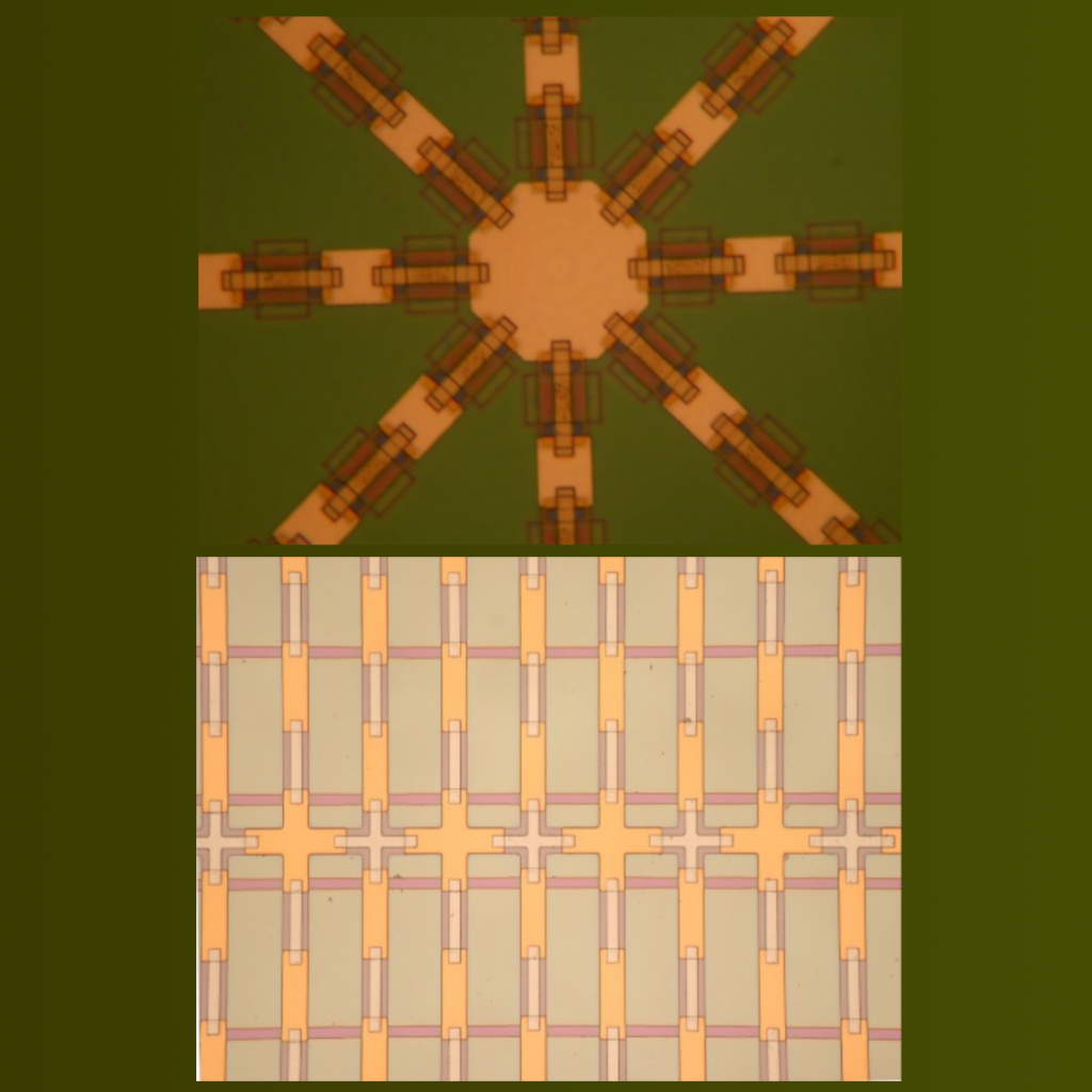
- Nano/microlitografia per la fabbricazione di dispositivi optoelettronici integrati (litografia e microscopia a fascio di elettroni, fotolitografia fronte-retro, litografia olografica)
- Processi di crescita, deposizione e attacco di film sottili per metalli, semiconduttori e isolanti in condizioni di ultra-alto vuoto (deposizione a fascio di elettroni e termica, sputtering, CVD, PECVD, RIE, processi di attacco umido e attacco elettrochimico, microlavorazione);
- Dicing e cleaving di wafer, lappatura e lucidatura, e incollaggio di dispositivi.
Caratterizzazioni Elettrottiche
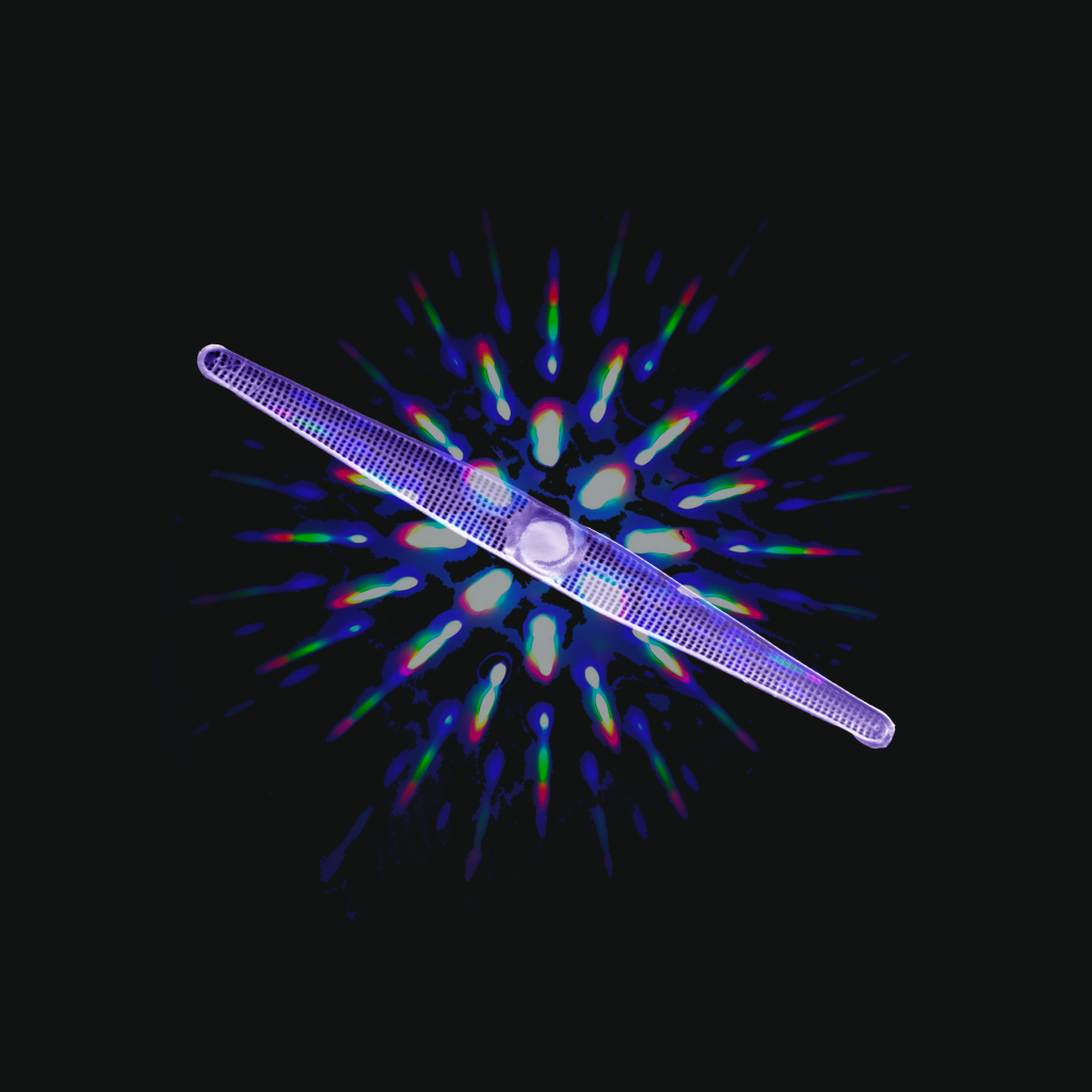
Configurazione elettro-ottica per la caratterizzazione lineare e non lineare di materiali, dispositivi e sistemi (laser continui, impulsi veloci, sintonizzabili, sorgenti supercontinuum, microscopi Raman lineari e non lineari, microscopia ottica in campo vicino a scansione SNOM, SEM, AFM, OSA, FTIR, diffusione dinamica della luce DLS, spettroscopia ellissometrica, spettrofotometri, monocromatori, set-up di misurazione della fotoluminescenza, misuratori di potenza, micromanipolatori, sistemi di posizionamento micro/nano, ecc.)
Bio-labs
- Facilities di biologia cellulare e molecolare (completamente attrezzate)
- Impianto Cnidaria (Hydra e Nematostella).
- Apparecchiature per istologia