Cryo Electron Microscopy laboratory “EYE LAB”
Unit of Naples
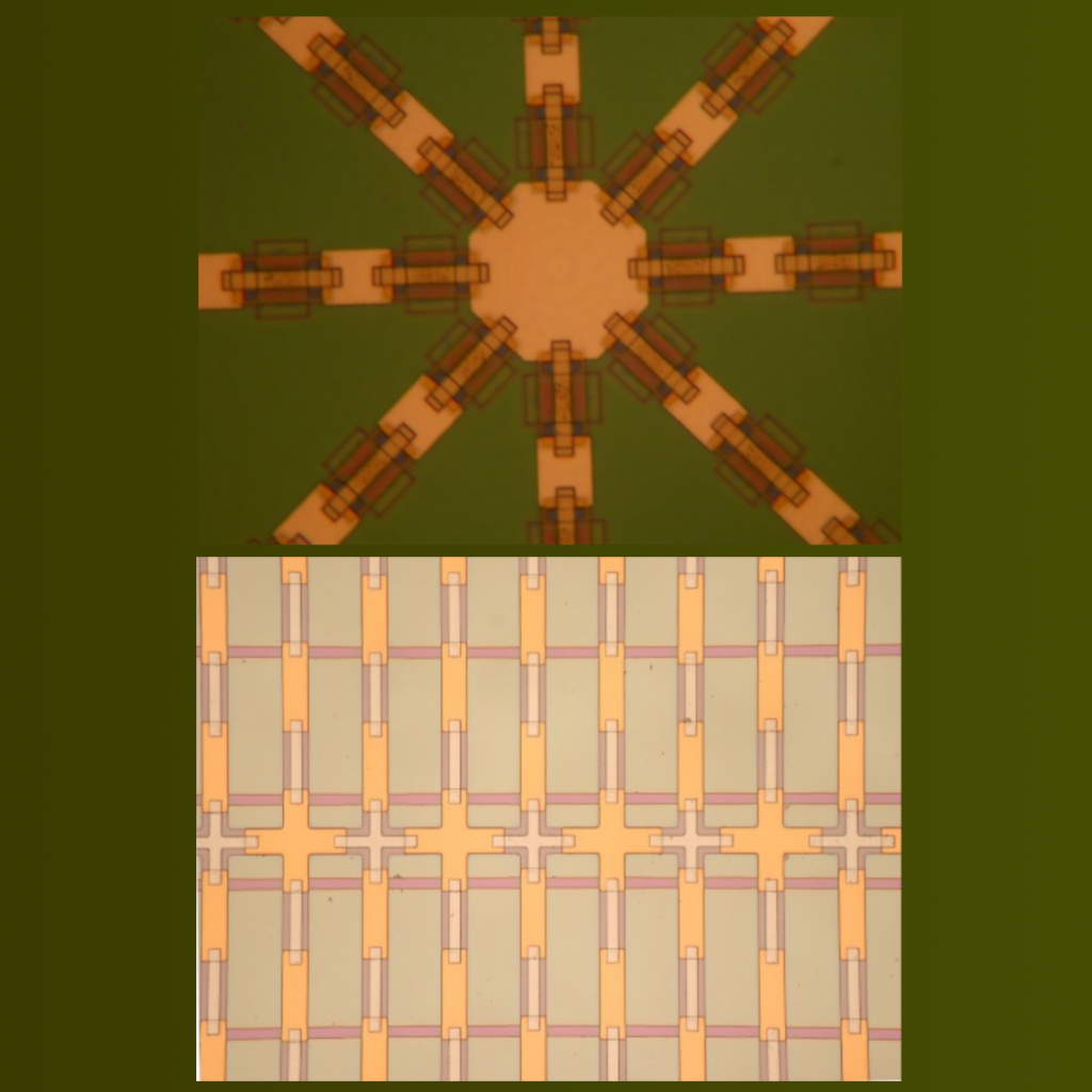
Micro-Nano Fabrication Laboratory ISASI Napoli (µNF Lab)
Unit of Naples

Pozzuoli Clean room
- Nano/microlithography for integrated optoelectronic device fabrication (electron beam lithography & microscopy, front-to-back photolithography, holographic lithography)
- Thin-film growth, deposition and etching processes for metals, semiconductors and insulators in ultra-high vacuum conditions (electron beam and thermal deposition, sputtering, CVD, PECVD, RIE, wet etching and electro-chemical etching processes, micromachining);
- Wafer dicing and cleaving, wafer lapping and polishing, device bonding.
Electro-optical characterization labs
Electro-optical set-up for linear and non-linear characterization of materials, devices and systems (continuous/fast pulsed/tunable lasers, supercontinuum sources, linear and non-linear Raman microscopies, SNOM-scanning near-field optical microscopy, SEM, AFM, OSA, FTIR, DLS-dynamic light scattering, ellipsometric spectroscopy, spectrophotometers, monochromators, photoluminescence measurement set-up, power-meters, micromanipulators, micro/nano positioning systems, etc)
Bio-labs
- Cell and molecular biology facilities (fully equipped)
- Cnidaria (Hydra and Nematostella) facility
- Histology equipments