Laboratory Manager: Mariano Gioffrè
The Naples Unit of ISASI features a state-of-the-art Micro/Nano Fabrication Clean Room that supports the development of nanotechnology, bio-sensing applications, photonic and microelectronic devices. Equipped with a wide range of micro and nano-scale device fabrication technologies, the Clean Room offers an ideal location for advanced technology research. It occupies an area of approximately 200 sqm and is maintained at class 100/1000 cleanliness levels to ensure the highest standards for research and experiments.
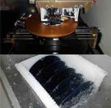
The Clean Room’s activities include fabricating optoelectronic devices, such as photodetectors, waveguides, optical sensors, and planar optical structures. It also focuses on developing solar-selective coatings suitable for Evacuated Flat Plate Solar Collectors (EFPC) technology. One of the unique features of the µNF facility is its focus on developing and fabricating photonic and optoelectronic devices using emerging graphene-like materials, particularly graphene and graphene oxide. Additionally, the facility specializes in the fabrication of microfluidic systems in poly (dimethylsiloxane) (PDMS) using soft lithography technique.
With oxidation and anneal furnace processing, PECVD deposition, sputter, e-beam and thermal evaporation, dry etching, wafer dicing, wet processing, and optical/laser lithography technologies, the Clean Room provides researchers with the necessary tools to conduct cutting-edge research
The µNF Lab is organized into three technological areas, each dedicated to a specific processing application: the Thin Film Lab, Wet Process Lab, and Optical Lithography Lab.
Thin Film Lab
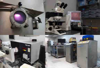
The Thin Film Lab is a 100 sqm laboratory specializing in thin film synthesis and etching processes. It is equipped with technologies for depositing III-V semiconductors, dielectric and metallic materials, as well as for thermal growth and annealing, and plasma dry etching processes. Equipment available includes PECVD systems, sputtering system, evaporators, and furnaces for annealing and oxidation. The TFL has recently acquired a new Deep RIE system with Bosch & Cryo option for etching high aspect ratio structures. The lab features an automated scribing/cleaving system, a metallographic microscope, and a stylus profilometer for post-process device analysis. In the near future, the TFL is expected to acquire a FEG-SEM microscope to further enhance its analytical capabilities.
Laboratory Manager: Mariano Gioffrè
Phone lab +39 81 61 32 723
Wet Process Lab
The Wet Process Lab focuses on wet processing and included a chemical bench for standard RCA procedures and wet chemical etching and lift-off processes. The lab also dedicated to electrochemical etching of silicon for the fabrication of porous silicon and fabrication of PDMS-based microfluidic chips. Recently, the lab has added the capability to deposit graphene onto a substrate using a solution-based process.
Laboratory Manager: Mariano Gioffrè
Phone lab +39 81 61 32 723
Optical Lithography Lab
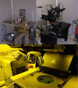
The Laboratory is a clean room with ISO 5 certification for Photolithography processes. It has a Mask Aligner with Bottom Side Alignment, an automated coating system, and a wet bench for developing. The lab also includes a refrigerator for storing photoresists and photosensitive polymers. A new laser writing system, the ML3 BabyPlus from Quantum Design, has recently been added, allowing high-resolution patterning down to 600 nm. It uses direct-write laser lithography for rapid prototyping of custom patterns without a photomask.
Laboratory Manager: Pia Dardano
Phone lab +39 81 61 32 723
Equipments List
Thin Film Lab
| Type | Model | Manufactures | Year | Processes |
| ICP-RIE system | PlasmaLab 80+ | Oxford Instruments | 2022 | ICP Etching – Deep Si Cryo Etching – Deep Si Bosch Etching |
| PECVD / RIE-ICP system | Custom | Angelantoni Industries | PECVD deposition of aSi:H, SiNx, SiOx RIE etching of Si, SiO2, Si3N4 – ICP etching of Si, SiO2, Si3N4 | |
| PECVD / RIE system | PlasmaLab 80 | Oxford Instruments | PECVD deposition of a.Si:H, SiNx – RIE etching of Si, SiO2, Si3N4 Surface activation by O2 plasma – Plasma Ashing by O2 plasma | |
| Magnetron Sputtering | LS 300 | Sistec | 1999 | Four cathode sputtering deposition Available Targets: a-Si, Al, Al2O3, Cr, Cr2O3, Er, ITO, Li3NbO4, NiCr, Si3N4, SiC, SiO2, Ti, ZnO. |
| e-Beam Evaporator | Custom | Sistec | 1999 | Metallization Process Thin film deposition of metals: Au, Al, Cu, Pd, Pt, Ag, Cr, Ni |
| Thermal Evaporator | Custom | EM Tecnoservices | Metallization Process Thin film deposition of metals: Au, Al, Cu, Pd, Pt, Ag, Cr, Ni | |
| Rapid Thermal Anneal Oven | RTP 600 | ModularPro | Rapid Thermal Annealing Temp. range 250°C to 1.300°C – Temp. Ramp Rate 1÷ 200 °C Wafer Size 2” ÷ 6 “ – Process Gas available O2, N2 | |
| Silicon Oxidation Oven | PEO 601 | ATV Technologie GmbH | Wet and Dry Silicon Oxidation Process gas available: O2, H2O, N2 – Temp. range 150°C to 1.100°C | |
| Metallographic Microscope | DM 6000 M | Leica | Morphological Characterization | |
| Scribing/Cleaving System | GST-150 | Dynatex | 2005 | Dicing Devices |
| Stylus Profilometer | P15 | KLA Tencor | Morphological Characterization |
Optical Lithography Lab
| Type | Model | Manufactures | Year | Processes |
| Mask Aligner | MA/BA6 | Karl Suss | Photolithography Resolution: Vacuum Contact <0.7μm – Hard Contact <1.0μm Soft Contact <2.0μm – Proximity (20 μm) <2.5μm | |
| Spin Coater | Delta 80 | Karl Suss | Photolithography | |
| Direct Laser Writing | ML3 BabyPlus | Quantum Design | 2023 | Lithography Maskless Integrated resolutions of 1 μm and 5 μm. Gray Scale mode with 256 levels for 3D patterning |