Description of the activity
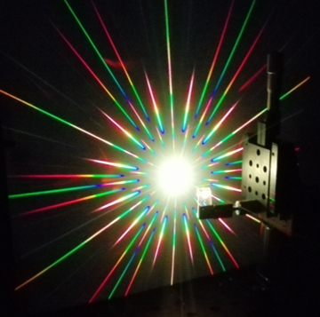
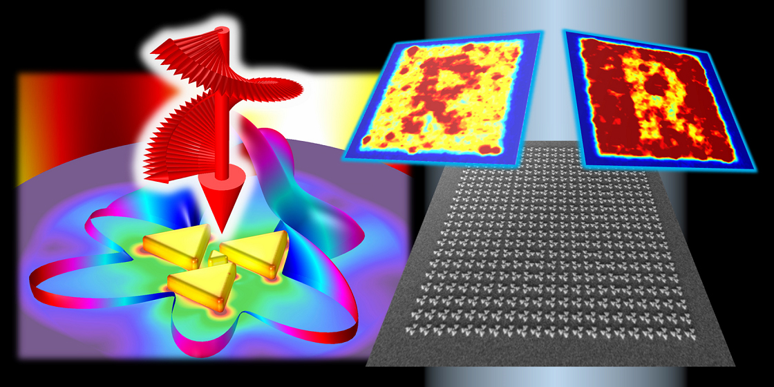
The Team has consolidated experience in the field of simulation and nanofabrication of photonic quasi-crystals (Thue-Morse, Octagonal and dodecagonal structures), and metamaterials, and fully equipped laboratories suitable for the preparation of such nanostructures. The structures are manufactured with a very high resolution electron beam lithography (EBL) process thanks to the Facility Raith 150, which is essential for obtaining excellent control of dimensions, shape, composition and configuration of plasmonic nanostructures. In detail, the manufacturing process comprises: 1) deposition on a suitable substrate of a polymeric material by means of a spin coating technique; 2) exposure of the substrate to the electron beam to transfer the designed pattern onto the polymer; 4) sputtering of metal films and post-processing by lift-off technique for the realization of gold nanostructures. The possibility of engineering complex metal nanoparticle arrays with distinctive plasmonic resonances extending across the entire visible spectrum can have a significant impact on the design and fabrication of novel nanodevices based on broadband plasmonic enhancement. With the use of PCs and PQCs, it is possible to synthesize novel artificial structures characterized by highly selective, sensitive, tunable in frequency EM response. We also design, simulate and fabricate octupolar, chiral nanostructures, reconfigurable and switchable metamaterials.
Involved personnel
M. Rippa | V. Marchesano | A. Vestri | D. Sagnelli | L. Petti
National and International Collaborations
- Prof. J. Zyss (ENS-Cachan, France),
- Prof. F. Simoni (Physics Dept. and Engineer of Materials of University of Marche),
- Prof. J. Zhou (Photonics dept. Of Ningbo University-China),
- Dr. Giuseppe Nenna (Nanomaterials and Devices Laboratory, Sustainable Materials Division, ENEA Portici Research Center),
- Prof. Antonio De Luca (Università della Calabria).
Instrumentation/facilities
The team coordinated by Dr. Petti in ISASI-CNR is equipped with:
- 1 IOL-integrated optics laboratory which includes a total of 1 fully equipped optical bench,
- 1 NanoFab-nanoFabrication laboratory with a clean room and fully equipped with a large Facility consisting of a Raith 150 electron beam lithography system,
- 1 NanoSOFT-Nanocomposites and Soft Matter laboratory for sample preparation,
- 1 SMART Materials laboratory (chemistry lab).
In these labs, characterized by an instrumental heritage of high technological value, take place the research activities of structured researchers, post-docs and researchers from other institutions operating in the field of biology and applied optics for non-destructive control and analysis of materials, laser-matter interaction, photonics and nano-fabrication, sensors and spectroscopy for the study and characterization of materials, as part of joint research projects.
The equipment and facilities available at ISASI-CNR include:
- NanoFAB: Clean room for nanolithography: Electron Beam Lithography system RAITH 150, Scanning Electron Microscope;
- IOL: Integrated optics laboratory: Laser sources form VIS to NIR: COHERENT laser source VERDI G5 (max power 5 W, λ=532 nm), NKT broad-band laser source SuperK COMPACT (λRange = 450 nm – 2400 nm), DPSS laser source 532nm-2W (CW), LD PUMPED ALL-SOLID-STATE BLUE LASER MBL- F-457 200mW, Optical light source @405nm-200 Mw; UV-VIS portable spectrometers Ocean Optics USB4000, UV-VIS portable spectrometers FLAME-T-VIS-NIR-ES Spectrometer Assembly 350-1000nm, Olympus Microscope BX51, Integrated Raman systems QEPro with optical microscopes @785nm, Integrated Raman systems NirQuest@1064nm (NIRQUEST512: NIR Spectrometer, 900-1700nm) with optical microscope; AFM-atomic force microscopy; 3D microfabrication technologies (microMake-Laser micromachining system and Wedge UV UV sub-ns DPSS @ 266nm); Optical set-up for: a) characterization of thin films, b) plasmonic resonances evaluation of metallic nanostructures and c) Far Field Diffraction analysis of periodic and a-periodic nanostructures. High resolution and computerized handling systems; Optical spectrum analyzers; Data acquisition and analysis systems.
- NanoSOFT: Soft Matter and Nanocomposites Lab: samples preparation laboratory: Spin coater CaLCTec FR10KPA, Laminar flow cabinet, Oven, optical microscope, hot stage, Quorum Sputterer, security cupboards for chemicals etc.
- SMART Materials Lab: In the Smart Materials lab, our task is to synthesize liquid crystal based materials and novel polymers. The infrastructures present in the lab are: Chemical fumehood equipped for simple synthesis, a rotovapor, a custom machine to prepare reactors cell, balance, security cupboards for chemicals.
Active projects and contracts
- H2OSafety Project: MIUR-PROOF OF CONCEPT- 467/Ric of 02.03.2018: “Design and development of environmental sensors for the research of microbiological and chemical contaminants hazardous to health (POC01_00109)”. Duration: 07/2019-01/2023. PI: L. Petti
- STADION Project: Photometric station for in vitro diagnostic analysis. ENEA External Fund (DFM.AD001.377) – contract