Descrizione dell’attività di ricerca:
The FET project concerns a new type of piezoelectric actuators (PZL) controlled by light using low-cost photo-mobile films (PMP) whose movement is induced and controlled by sunlight and/or artificial light. It aims to create a new class of photoactivable devices that could potentially change the current paradigms in a new field of piezo-phototronics by creating innovative devices for a wide range of applications such as Meso-scale machines Systems, Reconfigurable Optics Systems and Photoenergy Harvesting Systems.
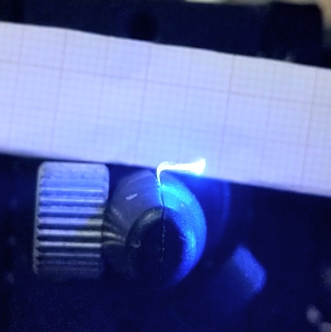
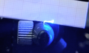
The main objective of this project is to study, simulate, fabricate and characterize actuators, sensors & harvesters that can be driven by light operating in the UV, VIS and NIR range to realize components and devices with different industrial goals combining Photo-mobile and piezo-materials. The present Concept/Principle relates to integrate an innovative light driven actuator (the PMP-PZL device) in opto-electronic systems for advanced industrial implementation. The project targets a novel and ambitious science and technological breakthrough as a first proof of concept in the new field of photo-activated piezoelectricity. Main technologies covered in PULSE-COM project combines piezoelectricity, photo-mobile excitation and semiconductors, which are the basis of piezotronic (piezoelectric-semiconductor coupling), piezophotonics (piezoelectric-excitation-photocell coupling), optoelectronics towards piezo-phototronics (piezoelectricity-semiconductors-photoexcitation).
Personale coinvolto:
D. Sagnelli | M. Rippa | V. Marchesano | A. Vestri | L. Petti
Collaborazioni Nazionali ed Internazionali:
- Dr. Giuseppe Nenna (Nanomaterials and Devices Laboratory, Sustainable Materials Division, ENEA Portici Research Center),
- Prof. Gustavo Ardila (Grenoble Alpes university),
- Prof. Thomas Skotnicki (Warsaw University of Technology),
- Dr. Maciej Haras (Warsaw University of Technology-CEZAMAT),
- Dr. Mateusz Wlazlo (CENTRUM BADAN I ROZWOJU TECHNOLOGII DLA PRZEMYSLU SPOLKA AKCYJNA (CBRTP S.A.),
- Dr. Frank Clayssen (CEDRAT TECHNOLOGIES SA (CTEC)).
Collaborazioni Nazionali ed Internazionali:
Attrezzature/strumentazioni:
The team coordinated by Dr. Petti in ISASI-CNR is equipped with:
- 1 IOL-integrated optics laboratory which includes a total of 1 fully equipped optical bench,
- 1 NanoFab-nanoFabrication laboratory with a clean room and fully equipped with a large Facility consisting of a Raith 150 electron beam lithography system,
- 1 NanoSOFT-Nanocomposites and Soft Matter laboratory for sample preparation,
- 1 SMART Materials laboratory (chemistry lab).
In these labs, characterized by an instrumental heritage of high technological value, take place the research activities of structured researchers, post-docs and researchers from other institutions operating in the field of biology and applied optics for non-destructive control and analysis of materials, laser-matter interaction, photonics and nano-fabrication, sensors and spectroscopy for the study and characterization of materials, as part of joint research projects.
The equipment and facilities available at ISASI-CNR include:
- NanoFAB: Clean room for nanolithography: Electron Beam Lithography system RAITH 150, Scanning Electron Microscope;
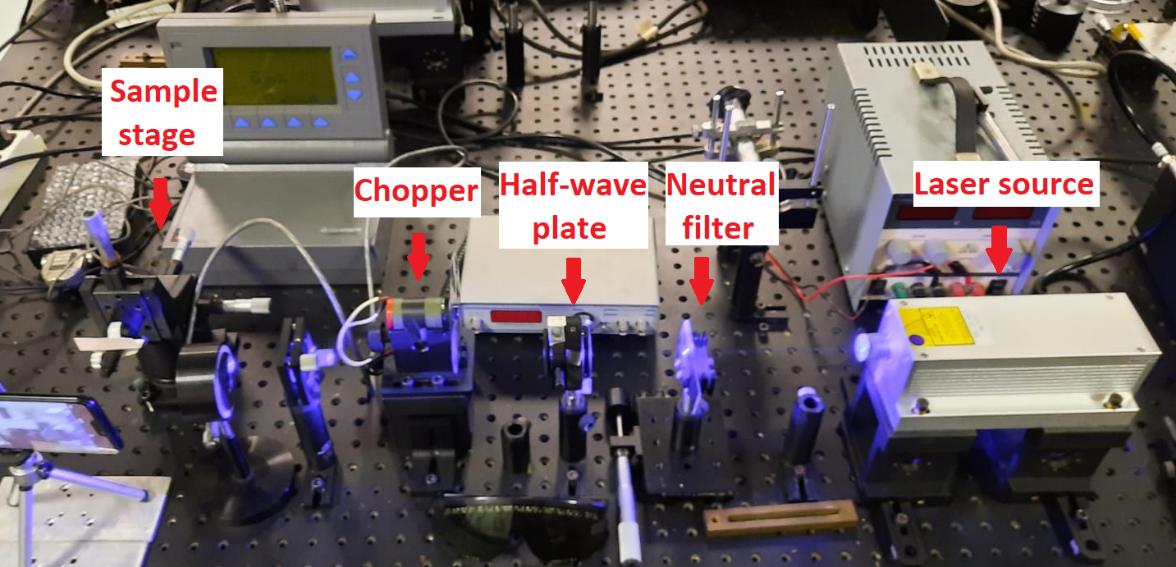
- IOL: Integrated optics laboratory: Laser sources form VIS to NIR: COHERENT laser source VERDI G5 (max power 5 W, λ=532 nm), NKT broad-band laser source SuperK COMPACT (λRange = 450 nm – 2400 nm), DPSS laser source 532nm-2W (CW), LD PUMPED ALL-SOLID-STATE BLUE LASER MBL- F-457 200mW, Optical light source @405nm-200 Mw; UV-VIS portable spectrometers Ocean Optics USB4000, UV-VIS portable spectrometers FLAME-T-VIS-NIR-ES Spectrometer Assembly 350-1000nm, Olympus Microscope BX51, Integrated Raman systems QEPro with optical microscopes @785nm, Integrated Raman systems NirQuest@1064nm (NIRQUEST512: NIR Spectrometer, 900-1700nm) with optical microscope; AFM-atomic force microscopy; 3D microfabrication technologies (microMake-Laser micromachining system and Wedge UV UV sub-ns DPSS @ 266nm); Optical set-up for: a) characterization of thin films, b) plasmonic resonances evaluation of metallic nanostructures and c) Far Field Diffraction analysis of periodic and a-periodic nanostructures. High resolution and computerized handling systems; Optical spectrum analyzers; Data acquisition and analysis systems.
- NanoSOFT: Soft Matter and Nanocomposites Lab: samples preparation laboratory: Spin coater CaLCTec FR10KPA, Laminar flow cabinet, Oven, optical microscope, hot stage, Quorum Sputterer, security cupboards for chemicals etc.
- SMART Materials Lab: In the Smart Materials lab, our task is to synthesize liquid crystal based materials and novel polymers. The infrastructures present in the lab are: Chemical fumehood equipped for simple synthesis, a rotovapor, a custom machine to prepare reactors cell, balance, security cupboards for chemicals.
Progetti e contratti attivi:
- PULSE-COM project. FET Horizon 2020 Grant agreement No 863227. Duration: 12/2019-07/2023. PI: L. Petti
- POC-PULSE Project: External investment for Photo-Piezo-Actuator implementation. Duration: 04/2022-10/2023 (1° Stage). Eureka External Fund